


 Material Insight: The Dielectric Constant of PCB Materials
 American Made Advocacy: What About the Rest of the Technology Stack?
 It’s Only Common Sense: Great Ideas From John Mitchell’s Book on Hiring Habits
Revolutionary X-Ray Microscope Unveils Sound Waves Deep Within Crystals
October 10, 2023 | SLAC National Accelerator LaboratoryEstimated reading time: 2 minutes
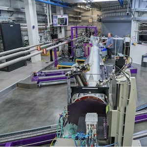
Researchers at the Department of Energy’s SLAC National Accelerator Laboratory. Stanford University, and Denmark Technical University have designed a cutting-edge X-ray microscope capable of directly observing sound waves at the tiniest of scales – the lattice level within a crystal. These findings, published last week in Proceedings of the National Academy of Sciences, could change the way scientists study ultrafast changes in materials and the resulting properties.
“The atomic structure of crystalline materials gives rise to their properties and associated ‘use-case’ for an application,” said one of the researchers, Leora Dresselhaus-Marais, an assistant professor at Stanford and SLAC. “The crystalline defects and atomic scale displacements describe why some materials strengthen while others shatter in response to the same force. Blacksmiths and semiconductor manufacturing have perfected our ability to control some types of defects, however, few techniques today can image these dynamics in real-time at the appropriate scales to resolve how those the distortions connect to the bulk properties.”
In this new work, the team generated soundwaves in a diamond crystal, then used the new X-ray microscope they developed to directly image the subtle distortions inside the crystalline lattice. They did so at the timescales at which these atomic-scale vibrations naturally occur by leveraging the ultrafast and ultrabright pulses available at SLAC’s Linac Coherent Light Source (LCLS).
The researchers placed a special X-ray lens along the beam diffracted by the crystalline lattice to filter out the “perfectly packed” portion of the crystal and zero in on distortions in the crystal's structure caused by the sound wave and defects.
“We used this to image how an ultrafast laser transfers its light energy into heat via successive reflections of the out-of-equilibrium sound wave off the front and back surface of the crystal.” Dresselhaus-Marais said. “By showing this in diamond – a crystal with the fastest sound speed – we illustrate the new opportunities now available with our microscope to study new phenomena deep inside crystals.”
The results identify a way to see super-fast changes in materials without damaging them. Before this discovery, the tools researchers used were much too slow to see these changes. This matters because many things, like how heat moves or how sound waves spread, depend on these fast changes.
The implications of this breakthrough stretch across various disciplines, from materials science to physics, and even extend to fields like geology and manufacturing. By understanding the atomic-level changes that lead to larger observable events in materials, scientists can get a clearer picture of transformations, melting processes, and chemical reactions in materials – accessing a new 13 orders of magnitude of timescales.
“This new tool offers us a unique opportunity to study how rare events caused by defects, atomic-distortions, or other localized stimuli inside a lattice give rise to macroscopic changes in materials,” Dresselhaus-Marais said. “While our understanding of the macroscopic changes in materials is rather advanced, we are often missing the details of which ‘instigating events’ ultimately cause the phase transformations, melting, or chemistry we observe at larger scales. With ultrashort timescales now at our fingertips, we have the ability to hunt for these rare events at their native timescales.”
Share on:


Suggested Items
Material Insight: The Dielectric Constant of PCB Materials
05/17/2024 | Dr. Preeya Kuray -- Column: Material InsightIn the world of PCB design, miniaturization can be achieved by using low dielectric constant (Dk) materials. Low Dk materials can allow for a reduction in thickness while maintaining a given trace width, leading to lower transmission loss and higher density circuitry.
IPC APEX EXPO: Some Thoughts About Growth
05/16/2024 | Dan Feinberg, I-Connect007After two and a half days of wandering the aisles at IPC APEX EXPO 2024, for the first time, I almost felt like I was exploring CES. There were so many booths and exhibits that I could describe, but I’d like to focus on the growth and huge value of this event, which has expanded well beyond just the growing and impressive exhibit show floor.
The Shaughnessy Report: Unlock Your High-speed Material Constraints
05/15/2024 | Andy Shaughnessy -- Column: The Shaughnessy ReportThe world of PCB materials used to be a fairly simple one. It was divided into two groups: the “traditional” laminates, often called FR-4, and the high-speed laminates developed especially for high-speed PCBs. These were two worlds that usually didn’t collide. But then traditional laminates started getting better, and high-speed designers and design engineers took notice and started to reconsider what FR-4 could be used for.
Breaking High-speed Material Constraints: Design007 Magazine — May 2024
05/14/2024 | I-Connect007 Editorial TeamDo you need specialty materials for your high-speed designs? Maybe not. Improvements in resins mean designers of high-speed boards can sometimes use traditional laminate systems instead of high-speed materials, saving time and money while streamlining the fab process. In the May 2024 issue of Design007 Magazine, our contributors explain how to avoid overconstraining your materials when working with high-speed boards.
Indium Experts to Present at Electronics in Harsh Environments SMTA Conference
05/13/2024 | Indium Corporationndium Corporation Technical Manager for Europe, Africa, and the Middle East, Karthik Vijay, will deliver a technical presentation and Indium Corporation Senior Technologist, Dr. Ronald Lasky, will deliver both a workshop and technical presentation at the Electronics in Harsh Environments SMTA Conference on May 14-16 in Copenhagen, Denmark.